
With global semiconductor demand expected to reach USD 1 trillion by the same year, India is positioning itself as a viable alternative in a world that currently depends heavily on Taiwan and South Korea for chip manufacturing, officials said.
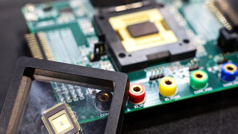
NEW DELHI – India has taken a major stride in its semiconductor journey with the launch of state-of-the-art 3-nanometre (nm) chip design facilities in Noida and Bengaluru. Inaugurated by Union Electronics and IT Minister Ashwini Vaishnaw, these advanced centers mark a significant leap in India’s design capabilities, placing the country among the few working at the cutting edge of chip innovation, according to an official statement released on Sunday.
“Designing at 3 nanometers is truly next-generation,” Vaishnaw said at the launch, noting that India had already achieved design expertise at the 7 nm and 5 nm levels. “This development marks a new frontier in semiconductor innovation,” he added. These are the first such facilities in India, signaling the country’s growing readiness to shift from being a chip consumer to an active contributor in global chip innovation and production.
This progress comes under the broader framework of the India Semiconductor Mission (ISM), launched in 2021 with a financial outlay of ₹76,000 crore. The mission aims to build a resilient and self-reliant semiconductor ecosystem by supporting chip fabrication, assembly, testing, packaging units, display fabs, and design startups.
India’s semiconductor market, currently valued at USD 45–50 billion, is projected to grow to USD 100–110 billion by 2030. With global semiconductor demand expected to hit USD 1 trillion in the same period, India is emerging as a credible alternative in a supply chain that has long depended on Taiwan and South Korea, officials stated.
The recent global supply chain disruptions have further emphasized the importance of geographic diversification in chip manufacturing, and India is increasingly viewed as a reliable partner in the global semiconductor arena.
The Ministry of Electronics and IT outlined key projects already in progress:
- Micron Technology is setting up an assembly and testing facility in Sanand, Gujarat, with an investment of ₹22,516 crore.
- Tata Electronics, in partnership with Taiwan’s Powerchip, is building a greenfield fabrication plant in Dholera, backed by an investment of ₹91,000 crore.
- Other approved projects include chip manufacturing units across Gujarat, Uttar Pradesh, and Assam by firms like CG Power, Renesas, HCL, Foxconn, and Kaynes Semicon.
Beyond infrastructure, the government is also actively supporting innovation through the Design-Linked Incentive (DLI) Scheme, which aims to nurture semiconductor design startups. So far, ₹234 crore has been approved for 22 startups developing chipsets for mobile networks, satellite communications, power management, and imaging systems. One DLI-supported startup is currently designing 3 nm chips using advanced Electronic Design Automation (EDA) tools.
To sustain long-term growth, building a skilled workforce remains a priority. Over 100,000 engineers are expected to be trained through SMART labs, with new partnerships formed with global technology leaders like Lam Research, IBM, and Micron, as well as academic institutions such as IIT Roorkee and Purdue University. One key collaboration aims to train 60,000 engineers over the next decade through simulation-based learning platforms.
India’s growing momentum will be on full display at the fourth edition of SEMICON India, scheduled for September, which is expected to attract participation from more than 300 global companies. With new milestones in chip design, strong investment in manufacturing infrastructure, and deep international collaboration, India’s semiconductor ambitions are rapidly becoming a reality.


Leave a comment